(Source: new PCB)
1. what is SLP
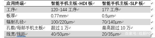
SLP(substrate-like PCB), abbreviated as carrier-like board (SLP) in Chinese, is the next generation of PCB hard board, which can shorten the line width/line spacing from 40/50 microns of HDI to 20/35 microns, I .e. the minimum line width/line spacing will be shortened from 40 microns of HDI to less than 30 microns of SLP. At present, Pengding Holding SLP can already achieve 25 microns. From the process point of view, SLP is closer to the IC carrier board used in semiconductor packaging, but it has not yet reached the specifications of the IC carrier board, and its use is still carrying a variety of active and passive components, so it still belongs to the category of PCB. With SLP boards for smartphones, the number of electronic components in the same area can reach twice that of HDI.
Comparison of HDI board and SLP board for smart phone
Opportunities for 2. SLP
Due to the development trend of intelligent, miniaturized and diversified functions of electronic products such as smart phones, tablet computers and wearable devices, the components that need to be carried on PCB have increased significantly, but the required size, weight and volume have been shrinking. In this context, the PCB wire width, spacing, the diameter and hole center distance of the microporous disk, and the thickness requirements of the conductor layer and the insulating layer are all declining, and the traditional HDI is limited by the process to meet the above requirements. Therefore, SLP technology with more stacked layers, smaller line width and line spacing, and more functional modules has become an inevitable choice to solve this problem.
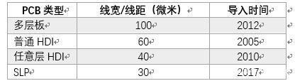
PCB line width/line spacing technology and import time evolution
With PCB with the same function, SLP can greatly reduce the area and thickness of HDI board, the thickness is reduced by about 30%, and the area is reduced by about 50%, which can make more space for electronic products to develop new hardware or increase battery capacity.
3. SLP technology
SLP adapts to SIP encapsulation technology, and a major improvement in SLP requirements lies in its fit with SIP encapsulation technology. According to the definition of the International Semiconductor Route Organization (ITRS), SIP(System in a Package) is a system-in-package technology. It is a single standard package that multiple active electronic components with different functions and optional passive devices, such as functional chips including processors, memories, MEMS and other functional chips and optical devices, are integrated into one package to realize certain functions, thus realizing a basically complete function, the packaging technology that forms a system or subsystem.
There are usually two ways to realize the function of electronic whole machine system, including unified single chip SOC(System on Chip) and systematic package SIP. SOC refers to the original different functions of the IC, integrated in a chip to achieve electronic system. In recent years, due to the increasingly difficult upgrading of semiconductor processes, the development of SOC has encountered technical bottlenecks, and SIP has become a new industrial technology trend in the electronics industry. For SIP, due to the high density of internal traces in the system-in-package, it is difficult for ordinary PCB boards to carry, while SLP is more suitable for the density requirements and is suitable for SIP packaging carrier.
4. SLP Manufacturing Technology
At present, in the printed circuit board and carrier board manufacturing process, there are mainly three process technologies: subtractive method, full-plus method and semi-plus method:
Subtractive method: subtractive method is the earliest traditional PCB process, but also the application of more mature manufacturing process, generally using photosensitive resist material to complete the pattern transfer, and the use of the material to protect the area does not need to be etched to remove, followed by acidic or alkaline etching solution to remove the copper layer in the unprotected area.
Full addition method (SAP): The full addition method process uses an insulating substrate containing a photosensitive catalyst, and after exposure according to the line pattern, the conductor pattern is obtained by selective chemical copper deposition.
Semi-additive method (MSAP): The semi-additive method is based on how to overcome the respective problems of the subtractive and additive methods in fine line production. The semi-additive method performs chemical copper on the substrate and forms a resist pattern thereon. The pattern on the substrate is thickened through an electroplating process to remove the resist pattern, and then the excess chemical copper layer is removed through flash etching. The area protected by the dry film and not thickened by electroplating is quickly removed in the differential etching process, and the remaining part forms a circuit.
Although SLP belongs to the printed circuit board, but from the process point of view, its line width/line spacing of 20 m/35 m, can not be used subtractive production, the same need to use MSAP process technology.
5. Apple is the market leader and leader of SLP
Apple leads the market towards SLP, which meets the requirements of high precision and SiP packaging technology: Apple's new products iphone and Apple Watch adopt "SLP"(SubstrateLike-PCB, referred to as SLP) technology with smaller line width and line spacing, leading the HDI market towards SLP, and technological upgrading brings new business opportunities to the industry. Since 2010, Apple's smart phones and tablet mainboards have adopted the Any Layer HDI process. In 2014, due to the continuous improvement of functions, new size and L-shape design, the industry has been booming. At present, Apple's adoption of SLP will accelerate the development of the board-like industry. However, due to the need to rebuild the board-like production line, the initial yield and quality need to be improved, and the leaders are expected to enjoy rich profit margins.
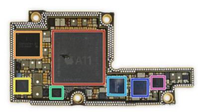
Apple has made extensive use of SiP packaging technology in products such as iPhone and Apple Watch. SiP technology has been used in iPhone6, and SiP accounts for 38% of iPhone X. At present, only Apple has used SLP in its products among the major mobile phone brands, including one SLP in Watch Series 4, two SLP in iphoneXS, and three SLP in Iphone XR MAX. It can be seen that the usage of SLP in Apple products is gradually increasing.
There are also constant reports that SLP will be adopted for Qida brand mobile phones and electronic products. However, as of the first half of 2019, most of the products actually launched have not yet adopted SLP, which is related to the difficulty of SLP production. At present, there are relatively few enterprises in the world that can supply SLP in bulk, and most of them supply to Apple. At present, Samsung and Huawei have begun to adopt SLP on a small number of high-end models of mobile phones. In any case, it is only a matter of time before the global high-end smart phones and other electronic products adopt SLP in bulk.
Global SLP Market Size and Forecast, 6.
According to the statistics of the new PCB Industry Research Institute, the market size of the global class carrier board (SLP) reached 6.7 billion billion yuan (nearly 1 billion US dollars) in 2018, and almost all of the market came from Apple. The global market size is expected to reach 10.4 billion billion yuan in 2019, up 54.68 percent year-on-year, accounting for 10.6 percent of the total PCB market size for mobile phones. In 2019, with the increase in the adoption rate of SLP, the core products of mobile phones and other mobile smart terminals of mainstream enterprises such as Samsung and Huawei, it is expected that by 2022, the global SLP market size will reach 27.4 billion billion yuan, accounting for 26.6 percent of the output value of PCB for mobile phones.
Major global SLP manufacturers in 7.
At present, the research and development and production lines invested in SLP mainly include Taiwan-funded enterprises Pengding Holdings, Taiwan Huatong, South Korea Samsung Motor (SamsungElectro- Mechanics), South Korea Circuit (Korea Circuit), South Korea Daeduck GDS, South Korea ISU Petasys, Japan Qisheng, Japan Il Feidian, Japan Mingxing, etc.

